
Information
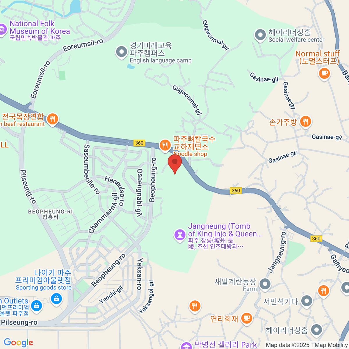
711 Pyeonghwa-ro, Tanhyeon-myeon, Paju-si, Gyeonggi-do, South Korea
-
-
-

Overview
- Summary
- A pioneering semiconductor assembly and test specialist in South Korea, providing various semiconductor components for electronic devices based on excellent semiconductor packaging and performance inspection technologiesA pioneering semiconductor assembly and test specialist in South Korea, providing various semiconductor components for electronic devices based on excellent semiconductor packaging and performance inspection technologies
- Key Products/Technologies
- Possession of diverse semiconductor packaging solutions, including Laminate Package, Lead Frame Package, and Flip Chip PackagePossession of diverse semiconductor packaging solutions, including Laminate Package, Lead Frame Package, and Flip Chip Package
- Application of technologies such as Fine Pitch Ball Grid Array (FBGA), Board On Chip (BOC), Stacked Die Chip Scale Package (SDCSP), Plastic Ball Grid Array (PBGA), Heat Spreader Plastic Ball Grid Array (HS-PBGA), Reinforced Plastic Ball Grid Array (RP-PBGA), and Fine Pitch Land Grid Array (FLGA) in laminate packagesApplication of technologies such as Fine Pitch Ball Grid Array (FBGA), Board On Chip (BOC), Stacked Die Chip Scale Package (SDCSP), Plastic Ball Grid Array (PBGA), Heat Spreader Plastic Ball Grid Array (HS-PBGA), Reinforced Plastic Ball Grid Array (RP-PBGA), and Fine Pitch Land Grid Array (FLGA) in laminate packages
- Flip-chip packages incorporate Flip Chip BGA (FCBGA) and Flip-Chip Chip Scale Package (FCCSP) technologiesFlip-chip packages incorporate Flip Chip BGA (FCBGA) and Flip-Chip Chip Scale Package (FCCSP) technologies
- Development of SiP (System in Package), Large Body, and Fine Pitch LAB technologies, along with the establishment of mass production systems for Advanced SiP modules and Recon Flip ChipDevelopment of SiP (System in Package), Large Body, and Fine Pitch LAB technologies, along with the establishment of mass production systems for Advanced SiP modules and Recon Flip Chip
- Provision of test program development, wafer probe, final test, burn-in, and other test support, as well as design and simulation servicesProvision of test program development, wafer probe, final test, burn-in, and other test support, as well as design and simulation services
- Capability in fingerprint sensor package technology developmentCapability in fingerprint sensor package technology development
- Core Advantages
- Over 50 years of accumulated experience and technological expertise as the first semiconductor assembly and test facility in South Korea since 1966Over 50 years of accumulated experience and technological expertise as the first semiconductor assembly and test facility in South Korea since 1966
- Excellent semiconductor packaging and performance inspection technologiesExcellent semiconductor packaging and performance inspection technologies
- Ability to timely develop and supply specialized products tailored to customer demands and semiconductor market conditionsAbility to timely develop and supply specialized products tailored to customer demands and semiconductor market conditions
- Capability to develop products with high reliability and superior thermal and electrical performanceCapability to develop products with high reliability and superior thermal and electrical performance
- Maintenance of technological competitiveness through continuous research and developmentMaintenance of technological competitiveness through continuous research and development
- Response to the next-generation packaging market through the development of SiP, Large Body, Fine Pitch LAB technologies and the establishment of Advanced SiP module and Recon Flip Chip mass production systemsResponse to the next-generation packaging market through the development of SiP, Large Body, Fine Pitch LAB technologies and the establishment of Advanced SiP module and Recon Flip Chip mass production systems
- Target Industries
- Communication marketCommunication market
- Consumer marketConsumer market
- Computer marketComputer market
- Automotive industryAutomotive industry
- Major Markets
- South Korea, China, Hong Kong, Japan, Singapore, TaiwanSouth Korea, China, Hong Kong, Japan, Singapore, Taiwan
- Certifications/Patents
- Possession of ISO/TS16949 certification for the automotive industryPossession of ISO/TS16949 certification for the automotive industry
- EIA599, SAC Level 1, QSS certification within Ford's TQEEIA599, SAC Level 1, QSS certification within Ford's TQE
- DESC, and NASA certificationsDESC, and NASA certifications
- Unique technological capabilities and know-how in semiconductor packaging and performance inspectionUnique technological capabilities and know-how in semiconductor packaging and performance inspection
- Continuous research investment for advanced packaging technology developmentContinuous research investment for advanced packaging technology development
Introduction
Location
711 Pyeonghwa-ro, Tanhyeon-myeon, Paju-si, Gyeonggi-do, South Korea
클릭하여 위치 살펴보기