


Information
231 Bangkkoji-gil, Seotan-myeon, Pyeongtaek, Gyeonggi-do, South Korea
+82 31-646-1515
-
Overview
- Summary
- Kostek Systems Inc. is a specialized company in semiconductor front-end and back-end equipment. A pioneer in the localization of Vacuum Cluster Tools. Possessing capabilities in Wafer Bonding Systems and Micro LED display manufacturing equipment development and supply. A key supplier of essential equipment for advanced semiconductor and display processes, including 3D TSV IC, Bump manufacturing, LED Chip, and smartphone camera CIS production.Kostek Systems Inc. is a specialized company in semiconductor front-end and back-end equipment. A pioneer in the localization of Vacuum Cluster Tools. Possessing capabilities in Wafer Bonding Systems and Micro LED display manufacturing equipment development and supply. A key supplier of essential equipment for advanced semiconductor and display processes, including 3D TSV IC, Bump manufacturing, LED Chip, and smartphone camera CIS production.
- Key Products/Technologies
- Vacuum Cluster Tools: Domestically developed semiconductor front-end process equipment.Vacuum Cluster Tools: Domestically developed semiconductor front-end process equipment.
- EFEM (Equipment Front End Module): Semiconductor wafer transfer and processing equipment.EFEM (Equipment Front End Module): Semiconductor wafer transfer and processing equipment.
- Load Port Module (LPM): Wafer cassette loading/unloading module.Load Port Module (LPM): Wafer cassette loading/unloading module.
- ATM ROBOT, Vacuum ROBOT: Automated wafer transfer robot systems.ATM ROBOT, Vacuum ROBOT: Automated wafer transfer robot systems.
- Wafer Bonding System: Diverse bonding systems including CIS Wafer Bonding System, Temporary Wafer Bonding System, Temporary Wafer De-Bonding System, and Temporary Wafer Bonding/Debonding System (TDBD). Model names TAURUS 300TB, TAURUS 300DB, TAURUS 300FOB, 300FOD included [database]. Achieving void-free uniform pressure control technology regardless of glue or film type adhesives and wafer flatness (TTV) precision of 3µm.Wafer Bonding System: Diverse bonding systems including CIS Wafer Bonding System, Temporary Wafer Bonding System, Temporary Wafer De-Bonding System, and Temporary Wafer Bonding/Debonding System (TDBD). Model names TAURUS 300TB, TAURUS 300DB, TAURUS 300FOB, 300FOD included [database]. Achieving void-free uniform pressure control technology regardless of glue or film type adhesives and wafer flatness (TTV) precision of 3µm.
- Plasma Ashing System: System for removing residues after semiconductor processes, including model R-7400.Plasma Ashing System: System for removing residues after semiconductor processes, including model R-7400.
- Encapsulation System: Encapsulation process system for protecting semiconductor chips.Encapsulation System: Encapsulation process system for protecting semiconductor chips.
- Vacuum Transfer System: Wafer transfer system in a vacuum environment.Vacuum Transfer System: Wafer transfer system in a vacuum environment.
- Micro LED Display Equipment: Micro LED display manufacturing equipment such as Chip Transfer System, Aligner & Pre-bonder, Thermal Eutectic Bonder, Laser Eutectic Bonder, and AR/VR Laser Eutectic Bonder. The Chip Transfer System offers a transfer yield rate of over 99.999% for 50um chip sizes and a spin coating uniformity of ±0.3%. The Aligner & Pre-bonder applies precise alignment of less than 2um and void-free bonding technology in a vacuum environment.Micro LED Display Equipment: Micro LED display manufacturing equipment such as Chip Transfer System, Aligner & Pre-bonder, Thermal Eutectic Bonder, Laser Eutectic Bonder, and AR/VR Laser Eutectic Bonder. The Chip Transfer System offers a transfer yield rate of over 99.999% for 50um chip sizes and a spin coating uniformity of ±0.3%. The Aligner & Pre-bonder applies precise alignment of less than 2um and void-free bonding technology in a vacuum environment.
- Micro OLEDoS Display Equipment: OLEDoS display manufacturing equipment including OCA/OCR Bonding System and Pol Lamination & Auto Clave System.Micro OLEDoS Display Equipment: OLEDoS display manufacturing equipment including OCA/OCR Bonding System and Pol Lamination & Auto Clave System.
- HBM Peel-off System: Equipment for removing adhesive film after the Through-Silicon Via (TSV) process in High Bandwidth Memory (HBM) manufacturing. Equipped with an auto splicer changer function and a heating chuck for removing high-adhesion films.HBM Peel-off System: Equipment for removing adhesive film after the Through-Silicon Via (TSV) process in High Bandwidth Memory (HBM) manufacturing. Equipped with an auto splicer changer function and a heating chuck for removing high-adhesion films.
- Core Advantages
- Securing technological leadership through the successful domestic development of Vacuum Cluster Tools.Securing technological leadership through the successful domestic development of Vacuum Cluster Tools.
- Possession of domestically developed Wafer to Wafer bonder and De-bonder technologies for next-generation semiconductor packaging (TSV, Fan-out).Possession of domestically developed Wafer to Wafer bonder and De-bonder technologies for next-generation semiconductor packaging (TSV, Fan-out).
- Localization of critical HBM (High Bandwidth Memory) manufacturing equipment, including Peel-off System and TDBD (Temporary Wafer Bonding/De-bonding) technologies, with differentiated features.Localization of critical HBM (High Bandwidth Memory) manufacturing equipment, including Peel-off System and TDBD (Temporary Wafer Bonding/De-bonding) technologies, with differentiated features.
- Independent technology development and product commercialization capabilities in the Micro LED and OLEDoS display equipment sectors.Independent technology development and product commercialization capabilities in the Micro LED and OLEDoS display equipment sectors.
- Strategic positioning as a strong equipment supplier for niche processes in future growth industries such as AI semiconductors, power semiconductors, and next-generation displays.Strategic positioning as a strong equipment supplier for niche processes in future growth industries such as AI semiconductors, power semiconductors, and next-generation displays.
- Accumulation of rapid development capabilities and technical know-how through a high proportion of R&D personnel (41-46%) and experienced professionals with over 10 years of tenure.Accumulation of rapid development capabilities and technical know-how through a high proportion of R&D personnel (41-46%) and experienced professionals with over 10 years of tenure.
- Technological validation through customer mass production evaluations and provision of differentiated features like auto splicer changers and heating chucks compared to competitors.Technological validation through customer mass production evaluations and provision of differentiated features like auto splicer changers and heating chucks compared to competitors.
- Achievement of void-free uniform pressure control technology regardless of glue or film type adhesives, and wafer flatness (TTV) precision of 3µm.Achievement of void-free uniform pressure control technology regardless of glue or film type adhesives, and wafer flatness (TTV) precision of 3µm.
- Target Industries
- Semiconductor Industry: Semiconductor front-end and back-end processes, 3D TSV IC, Bump manufacturing, HBM (High Bandwidth Memory), and power semiconductor manufacturing processes.Semiconductor Industry: Semiconductor front-end and back-end processes, 3D TSV IC, Bump manufacturing, HBM (High Bandwidth Memory), and power semiconductor manufacturing processes.
- Display Industry: LED Chip manufacturing, smartphone camera CIS manufacturing, Micro LED display, and OLEDoS display manufacturing processes.Display Industry: LED Chip manufacturing, smartphone camera CIS manufacturing, Micro LED display, and OLEDoS display manufacturing processes.
- Electric Vehicle and Renewable Energy Industries: Supply of sinter bonder equipment for high-efficiency power semiconductor manufacturing.Electric Vehicle and Renewable Energy Industries: Supply of sinter bonder equipment for high-efficiency power semiconductor manufacturing.
- Major Markets
- South KoreaSouth Korea
- Certifications/Patents
- Possession of 'Materials, Parts, and Equipment (SooBuJang) Strong Company' designation certificate.Possession of 'Materials, Parts, and Equipment (SooBuJang) Strong Company' designation certificate.
- Possession of 'SooBuJang Core Strategic Technology' confirmation certificate.Possession of 'SooBuJang Core Strategic Technology' confirmation certificate.
- Acquisition of RWTUV certification.Acquisition of RWTUV certification.
- Securing various international certifications including CE(EMC), CE(LVD), FCC(wireless communication), IC(wireless communication), IECEE, NRTL, SRRC(wireless transmission equipment), TELEC, and VCCI.Securing various international certifications including CE(EMC), CE(LVD), FCC(wireless communication), IC(wireless communication), IECEE, NRTL, SRRC(wireless transmission equipment), TELEC, and VCCI.
- Operation of a patent status page on the official website.Operation of a patent status page on the official website.
Introduction
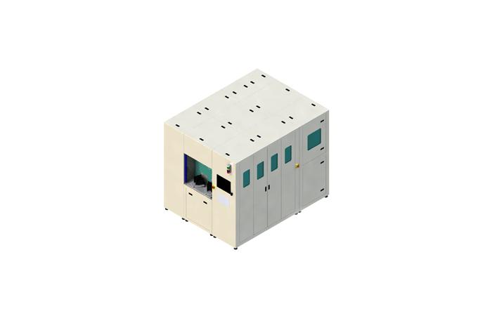
Key Products


Location
231 Bangkkoji-gil, Seotan-myeon, Pyeongtaek, Gyeonggi-do, South Korea
클릭하여 위치 살펴보기
